home                 consulting                products & tools                 clients                 about 


logo


(781) 454-7648
  info@RockfieldResearch.com
PCB2STL  -  3D Printed Circuit Boards
    Printed circuit board (pcb) fabrication software generates a standard format output - Gerber files (also called photoplot files).  These are used by pcb manufacturers industry wide.

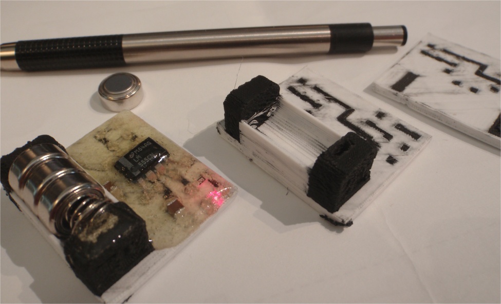
     Graphene 3D Labs has perfected a highly conductive plastic fiber suitable for 3D printing.  Now, with a dual head 3D printer, you can 3D print circuit boards right from the output of standard pcb layout software.   PCB2STL is a tool that links the two manufacturing processes for you.

      Your pcb layout software should produce a gerber file for each layer -- these include each conductor layer as well as other fabrication details such as solder mask and silkscreen images.   PCB2STL will convert a gerber file for the image of one conductor layer into two STL files readable by 3D slicer software. 

       Thanks to Graphene 3D Labs, this software is free for you to use!

______________________________________________________________________________________________

click to download PCB2STL

This software is experimental, and is work in progress.  As of May 2015, this has only been tested under very limited conditions:  
operating system:                      Windows 7 Pro 64
source of Gerber file input:       PADS Layout v9.3.1
interpreter of STL file output:   Simplify3D v2.2.2
dual head 3D printer:                FlashForge Creator Pro

Please refer to the example below -- this version is limited to certain Gerber file geometries.  This software remains the property of Rockfield Research Inc.  We grant each downloader the use of the executable for the purposes of expanding the application of Graphene 3D Labs conductive fiber.  This software is provided with absolutely no warranty.  Use at your own risk.

We are very interested in hearing about your successes, your problems, or your ideas relative to PCB2STL.  We will attempt to update PCB2STL to incorporate suggestions, as well as to fix bugs you find.  Email us here.

LIMITS:   This version is preliminary, and does not yet have full features.  At present, it will only work correctly for square or rectangular pads (not circular or more complex shapes).  All pad edges and traces must be rectilinear - no curves or diagonals.  Assumptions are made regarding units -- it is assumed that the Gerber file dimensions are in inches/mils, future upgrades will read the file metadata and properly convert.  Output of STL files is in mm.  The STL files generated have not been reduced to eliminate intersecting structures - some slicer software may generate errors on this or not correct it properly.


______________________________________________________________________________________________
A worked example:

Our first demonstration was a simple LED flasher using the ubiquitous 555 timer chip.   Our experiments showed that we could reliably make circuits with "spaces and traces" of at least 0.050-0.070" size.  We chose a DIP package for the 555 timer and flared out the pins a bit to generate larger clearances.  We chose 1206 and 1210 size surface mount components for the passive elements, and expanded the pads outwards a bit for additional clearance.

Step 1:  We generated the schematic using PADS Logic (view).

Step 2:  We transferred the schematic to PADS Layout.  We maintained generous clearances in routing the layout.  We planned this as a "2 layer pcb", with only the ground and +V buswork on the bottom layer.  (view).  (Note that we brought out the power buswork to the left - we will hook this up to a battery structure in a bit.)

Step 3:  Manage the layers -- in a conventional circuit board, the 2 layers would be connected by plated-through holes.  Here, we must make 3 layers of conductors, with the mid-layer being "columns" of conductor where the plated holes should be.  This results in a 3-layer board, with this stackup (view).

Step 4:  Mark the corners -- Note that on each layer, we have small "L" fiducials to mark the corners.  This will help later, as the slicer software wants to "auto-adjust" the locations of STL files, and it helps to make sure that each layer will generate STL files with the same dimensions.

Step 5:  Generate the photoplot files.  We generated three:   C1.pho, C2.pho, and C3.pho   (top, middle, bottom).

Step 6:  Run PCB2STL for each Gerber photoplot file.  For each, we must specify the base elevation, thickness, and select one of the files.  Starting at the bottom and working our way upwards, we selected:
file   C3.pho                 elevation = 0.0 mm                    thickness = 0.8 mm
file   C2.pho                 elevation = 0.8 mm                    thickness = 0.8 mm
file   C1.pho                 elevation = 1.6 mm                    thickness = 0.8 mm

This will generate six STL files, two for each run.  The conductor structures are in C1_CND.stl, C2_CND.stl, and C3_CND.stl, while the insulator structures are in C1_INS.stl, C2_INS.stl, and C3_INS.stl.

Step 7:  Import STL files to a Slicer utility.  We used Simplify3D for this.  Since we specified the elevations and thicknessess carefully and marked all the corners, Simplify3D will automatically align all six STL files correctly into a solid 3D structure.  Otherwise, we have to manually edit the offsets for each element.

Step 8:  Add mechanical structures.  For our example, we added four elements which were drawn in Solidworks.  One was an extra base plane under the bottom layer, to provide a solid insulator layer for good 3D printing adhesion.  The other three make a battery holder, suitable for three type 357 (1.55V) batteries with the use of a spring clip (such as Digikey part BCAAA-ND).

Step 9:  Finish the setup.  Associate each imported structure with the correct process (i.e. which printer head and what printing parameters to use).  This will differ with different slicer software - for Simplify3D we defined conductor and insulator processes with our best printing parameters for graphene PLA and normal PLA fiber.    (download the complete printable "job" for Simplify3D).

Step 10:  Print it!

Step 11:  Assemble the circuit.  We used silver conducting epoxy to "solder" the components to the pads.  Since this stuff is not so strong structurally, we protected the finished circuit with standard 5-minute epoxy.

flasher image

_________________________________________________________________________________________________________

optics                   electronics                  controls                big data                  contact